Students awarded prizes for their class designs of an energy harvesting circuit and a high efficiency audio amplifier
The two winning teams designed an energy harvesting circuit for implantable devices and sensor networks, and a high efficiency audio amplifier for mobile applications.
Two teams in the Fall 2011 EECS 413 (Monolithic Amplifier Circuits) Design Contest came up with winning designs for their final class project: an energy harvesting circuit for implantable devices and sensor networks, and a high efficiency audio amplifier for mobile applications.
Each year Prof. Michael Flynn adds to the students’ motivation by arranging for an in-class contest that is sponsored by industry. Thanks to this year’s sponsorship by Cirrus Logic, the students will share prize money in the amount of $3K.
First place
A Battery-Less Thermoelectric Energy Harvesting Circuit Using a 75mV Source
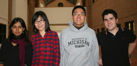
Design by iran Alhaideri (UG EE), Tony Chen (UG EE), Yutian Lu (Grad EE), Daksha Sharma (Grad EE)
 Enlarge
The team described their project:
Background
Energy is becoming one of the major constraints in many modern applications such as implantable biomedical devices and Ubiquitous Sensor Networks (USN). Conventional power supplies such as batteries are not always the best option when battery-replacement is difficult to manage. As power consumption of CMOS circuits continues to decrease, energy harvesting from various sources as a replacement for batteries is becoming a more viable option.
Project
 Enlarge
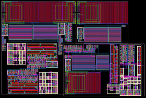
Our team implemented an energy harvesting circuit that interfaces with a thermoelectric generator (TEG), a device used to convert temperature gradients into electric potential at 25 mV/K. The energy provided from our circuit could be used to directly power body-wearable devices by using the temperature gradient between the human body and environment. Our project was designed to work with a 3 K temperature difference, corresponding to a 75 mV source.
Our design utilized three separate submodules to boost VDD up to 1.8 V and store the excess energy onto a capacitor for later use. Through the use of two boost converters and a buck converter, we were able to regulate an output voltage to 1V that is independent of the external load. This design used digital control to achieve zero-current switching – improving the maximum system efficiency.
Our design utilized a 0.13 μm CMOS technology and had a die area of 0.0338 mm2. The system was able to provide up to 100 uW of power with a maximum efficiency of 40%.
Second Place
Closed-Loop Uniform PWM Class-D Audio Amplifier with -108dB THD
Design by Bjorn E. Grubelich (Grad EE), Yonggang Ma (Grad EE), Jing Hu (Grad EE), Chia-Hsiang Chen (Grad EE)

 Enlarge
The team described their project:
Background
The Class-D audio amplifier provides significant advantages over Class-A, Class-B, and Class-AB audio amplifiers in many applications because the lower power dissipation produces less heat. As a result, a growing demand for high efficiency audio amplifiers in mobile applications has motivated the Class-D’s ubiquity in sub-micron CMOS technology.
Project
 Enlarge
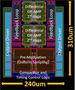
Aside from power efficiency, the desire for high power supply rejection ratio (PSRR) and low total harmonic distortion (THD) has furthered the development of closed-loop Class-D architectures. This project employs a closed-loop architecture to achieve higher PSRR, lower THD, and higher SNR. The fixed closed-loop gain provided by the global feedback provides the added benefit to against noise from process variation, supply jitter and temperature fluctuation. This circuit is implemented in 0.13 μm CMOS technology with a 0.075mm2 core area and the measured THD can be as low as -108dB while the SNR is 117dB.
Reflections about the project
This was our first attempt at designing a fully-differential closed-loop Class-D audio amplifier. As we learned more from EECS 413, we identified various design challenges such as stability, frequency compensation, and feedback. By integrating the pulse-width modulation and filtering blocks into a closed-loop system we achieved high performance with acceptable power consumption. Although the system architecture was quite complex and frustrating at times, this was a great experience that made us better analog designers.

 MENU
MENU